Circuit Design with KiCad
From schematic to PCB layout in one session
2 hours
8 per session
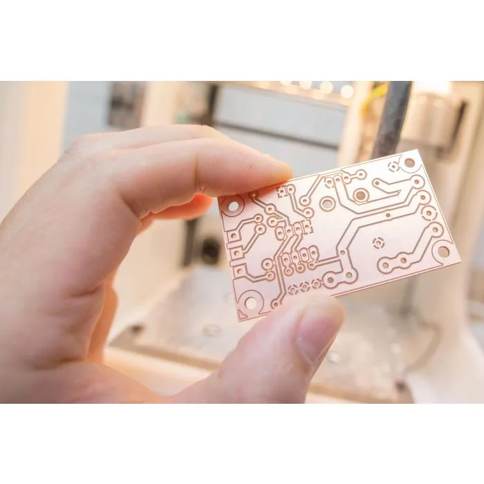
You'll use KiCad to design a complete circuit — from schematic capture through component placement to routed PCB. By the end you'll have a board file ready to send to a fab house. We work through a real project so you learn the workflow, not just the menus.
What you'll learn
- >> Create schematics with proper symbols, nets, and power rails
- >> Assign footprints and generate a netlist for PCB layout
- >> Place components and route traces with good design practices
- >> Run design rule checks and generate Gerber files for manufacturing
Register your interest
No sessions are currently scheduled. Let us know you're interested and we'll notify you when new dates are announced.
We'll let you know when new sessions are announced.
Thanks! We'll let you know when sessions are announced.
Built on six principles
Passionate
We love what we do — and that makes us better at teaching it.
Credible
Real skills, real outcomes — delivered on leading brands and platforms.
Welcoming
Everyone starts somewhere. We make starting easy.
Hands-on
Real doing at the heart of every experience.
Structured
Every session has a plan. Every participant leaves with a result.
Innovative
The tools, platforms, and techniques the industry uses today.